






The insightful articles, inspiring narrations and analytical perspectives presented by the Editorial Team, establish an alluring connect with the reader. My compliments and best wishes to SP Guide Publications.

"Over the past 60 years, the growth of SP Guide Publications has mirrored the rising stature of Indian Navy. Its well-researched and informative magazines on Defence and Aerospace sector have served to shape an educated opinion of our military personnel, policy makers and the public alike. I wish SP's Publication team continued success, fair winds and following seas in all future endeavour!"

Since, its inception in 1964, SP Guide Publications has consistently demonstrated commitment to high-quality journalism in the aerospace and defence sectors, earning a well-deserved reputation as Asia's largest media house in this domain. I wish SP Guide Publications continued success in its pursuit of excellence.
The Dholera project represents India's ambition to walk before it runs, recognising that semiconductor success is a marathon spanning decades
 |
The Author is Former Director General of Information Systems and A Special Forces Veteran, Indian Army |
India's quest for semiconductors is rapidly shifting from a vision to reality, driven by a massive ₹76,000 crore ($8 billion) push through the India Semiconductor Mission (ISM). By building domestic fabrication, assembly, and design infrastructure, India aims to de-risk global supply chains and achieve 75 per cent self-sufficiency in domestic chip demand by the year 2029.
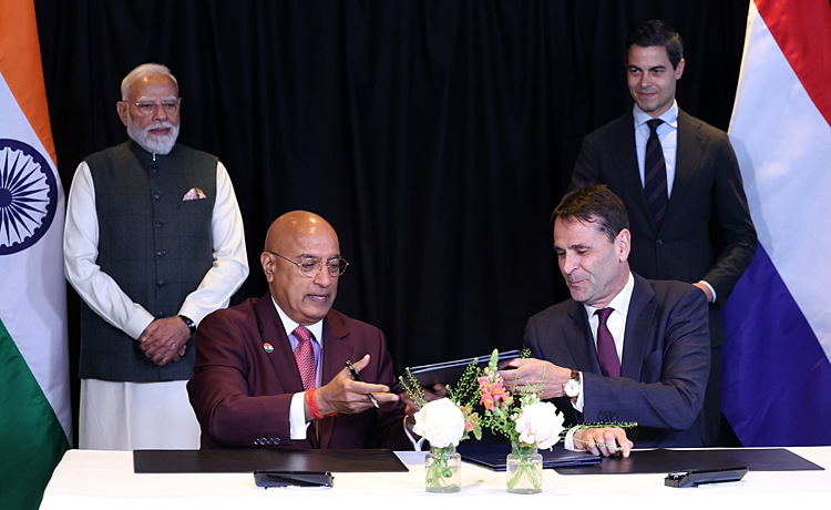
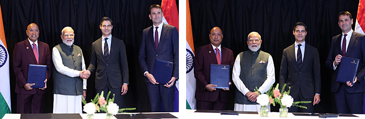
On May 16, 2026, Prime Minister Narendra Modi, accompanied by Dutch Prime Minister Rob Jetten, witnessed the signing of a landmark agreement between TATA Electronics and Netherland's firm Advanced Semiconductor Materials Lithography (ASML) at ASML's headquarters in Veldhoven, Netherlands.The partnership between the two companies is expected to accelerate India's integration into global semiconductor supply chains and reduce dependence on imports.
India's choice reflects pragmatism. It is building for the chips its economy actually consumes, not the ones that dominate headlines.
ASML is a global leader in high precision lithography equipment, which is indispensable in the production of semiconductor chips. The US semiconductor production relies heavily on ASML cooperation. TATA Electronics, a subsidiary of the TATA Group, is spearheading India's semiconductor ambitions by establishing the Dholera facility, which will be a cornerstone of the country's technological self reliance. The announcement of TATA Electronics ₹91,000-crore semiconductor fabrication facility at Dholera, Gujarat, marks a decisive moment in India's industrial and technological trajectory.
ASML, the sole manufacturer of extreme-ultraviolet lithography machines, committed to supplying lithography systems, technical training and ecosystem support for India's first commercial fab, which is being built in collaboration with Taiwan's Powerchip Semiconductor Manufacturing Corporation (PSMC). The facility is expected to produce its first saleable wafers by late 2026.
Instead of chasing the cutting edge of 3nm or 2nm technology, the Dholera fab will focus on 28nm chips, with additional capacity for 40, 55, 90 and 110nm nodes. These mature nodes are the backbone of automotive electronics, power management systems, telecom radios, industrial sensors and embedded silicon. Roughly 70 per cent of global wafer volume sits at 28nm and above, while only 3 per cent lies at 3nm and below. India's choice reflects pragmatism: it is building for the chips its economy actually consumes, not the ones that dominate headlines.
Significantly, all successful semiconductor nations began at the trailing edge of its era and climbed gradually. The Taiwan Semiconductor Manufacturing Company Limited (TSMC) began with 3 microns in 1987 and took 35 years to reach 3nm. China's Semiconductor Manufacturing International Corporation (SMIC) began at 180nm in 2000 and only reached 7nm-class production in 2023 after massive state subsidies.
By choosing 28nm, India has arrived at the starting line of a 30-year journey. The chips India actually needs are the ones Dholera will produce
Moreover, Singapore's Chartered Semiconductor and Malaysia's Silterra, which either chased the leading edge prematurely or stagnated at the trailing edge without anchors, failed to sustain competitiveness. India's earlier attempts (from the SCL fab at Mohali to the SemIndia and Jaypee-IBM ventures) collapsed due to lack of market demand or financial closure.
However, the market has since transformed, driven by smartphones, electric vehicles (EVs), defence electronics and geopolitical decoupling from China. Notably, 28nm fab costs between $10–15 billion to establish, compared to $20 billion for 3nm and $28 billion for 2nm. ASML's High-NA EUV scanners, essential for sub-7nm production, cost $380 million each, weigh as much as two Boeing 777s and take six months to install.
In terms of demand, Tokyo-based Renesas Electronics (semiconductor company that specialises in embedded processing, analog, power, and connectivity solutions) launched its flagship automotive microcontroller at 28nm in March 2026. The US Bureau of Industry and Security found that 80 per cent of chips in modern cars sit between 28 and 180nm. A single passenger vehicle contains between 1,400 and 3,000 chips, and the 2021 global auto crisis was caused by shortages of 28–90nm microcontrollers, not 3nm processors. Maruti Suzuki alone cut production by 51 per cent in September 2021, costing the Indian auto industry around ₹25,000 crore in lost sales. By choosing 28nm, India has arrived at the starting line of a 30-year journey. The chips India actually needs are the ones Dholera will produce.
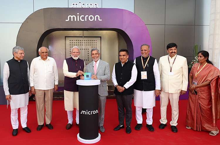
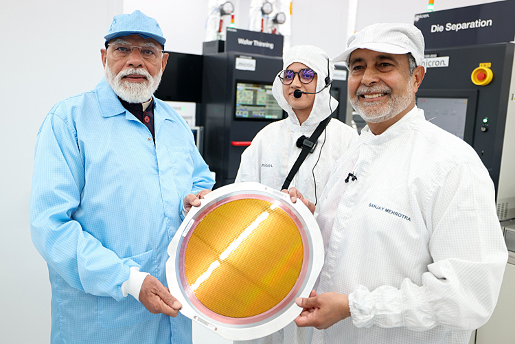
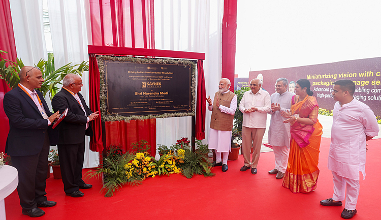
India's ecosystem is being assembled in parallel. TATA's Outsourced Semiconductor Assembly and Test (OSAT) facility at Jagiroad, Micron's Sanand plant inaugurated in February 2026, CG Power–Renesas at Sanand and Kaynes Semicon's operations since March 2026 provide the back-end support for packaging, testing and integration.
By the time Dholera's wafers roll out, India will have a complete supply chain to absorb them. This marks a sharp departure from earlier failures where fabs were proposed without a domestic market or supporting ecosystem
By the time Dholera's wafers roll out, India will have a complete supply chain to absorb them. This marks a sharp departure from earlier failures where fabs were proposed without a domestic market or supporting ecosystem.Analysts; however, point out execution gaps, noting that only 15 per cent of the Design-Linked Incentive scheme's FY24 budget was disbursed. China's Big Fund-III is deploying $47 billion at 28nm, with SMIC already slashing wafer prices to flood the market.
The US imposed a 50 per cent tariff on Chinese semiconductors in January 2025, with further increments due in 2027, while Section 5949 of the US National Defense Authorization Act (NDAA) will bar federal contractors from using Chinese chips in critical systems from December 2027. America may soften its stance towards Beijing in the aftermath of US President Donald Trump to China, but not much in semiconductors. This is advantage to India, which is emerging as a credible alternative.
The Dholera fab will directly support India's electronics industry, which imported components worth ₹34,000 crore last year. The project represents India's ambition to walk before it runs, recognising that semiconductor success is a marathon spanning decades. This fab is expected to ramp to full capacity by 2028, creating over 20,000 jobs and anchoring a supplier ecosystem for gases, chemicals and packaging.
All this is good development but we must understand that ASML does not produce microchips itself. Instead, it designs and manufactures the critical photolithography machines (such as Extreme Ultraviolet or EUV systems) that foundries like TSMC, Samsung, and Intel use to print circuits for 3nm and 2nm chips. ASML holds a global monopoly on the EUV equipment required to manufacture 3nm and 2nm logic chips. Their tools use short-wavelength light to print microscopic circuit patterns onto silicon wafers. For the latest 2nm node processes, ASML produces next-generation "High-NA EUV" systems (such as the EXE:5200). These machines offer higher resolution and allow foundries to fit more transistors onto a single chip.
3nm and 2nm semiconductor nodes deliver massive leaps in processing power and battery life by packing billions more transistors into the same physical space. The primary benefits include unprecedented energy efficiency, reduced power leakage, and the computational muscle required for next-generation artificial intelligence (AI) and 5G.
Finally, while we are whitewashing the issue by saying that instead of chasing the cutting edge of 3nm or 2nm technology, we are going in for 28nm chips, it can be safely assumed that sub-5nm technology has not been offered by ASML to India, which is in line with the Western approach of denying critical technology to India.